Nanocomposites and Manufacturing Technology
§ 1. Scalable micro/nano-manufacturing using Shear-induced Interfacial Instability

This project investigates the spontaneous pattern generation by ribbing instability in an ordered manner using a fundamentally new approach to manufacture three-dimensional micro and nano-scale structures on a large-area substrate. One of the applications is hydrodynamic drag reduction. A technology that can reduce the friction or drag on ship hulls would have a substantial economic and environmental impact by improving fuel efficiency (Fig. 1). Microstructured superhydrophobic surfaces may retain air pockets that can act as gas lubrication between the water and the ship hull. Although the superhydrophobic surfaces have been studied for nearly two decades, it is only recently that periodic linear-trench structures (Fig. 2) have been shown to be effective for marine crafts traveling in open water, which represents the sea, oceans, and lakes. The manufacturing of such well-defined micro-trenches has relied on silicon-based microfabrication based on semiconductor manufacturing approaches. These silicon processes are prohibitively expensive and not scalable for large surface areas, such as ship hulls.
This study demonstrates a simple template-free scalable manufacturing technique to fabricate periodic microstructures by controlling the ribbing instability in the forward roll coating (Fig. 3). Viscoelastic composite coating materials are designed to achieve a controllable ribbing with a periodicity of 114–700 µm. The periodic microstructure enables superhydrophobicity. When towed in a static water pool, a model boat coated with the microstructure film shows 7%–8% faster speed than the boat with a flat control film. The CNT addition shows both mechanical and electrical properties improvement (Fig. 4).
Reference
, , , , , , , , , , , , , , Template-Free Scalable Fabrication of Linearly Periodic Microstructures by Controlling Ribbing Defects Phenomenon in Forward Roll Coating for Multifunctional Applications. Adv. Mater. Interfaces 2022, 2201237. https://doi.org/10.1002/admi.202201237
§ 2. Nanomanufacturing and Nanocomposites for Metamaterials
A metamaterial is a material engineered to have a property that is not found in nature. They are made from assemblies of multiple elements fashioned from composite materials such as metals or plastics. The materials are usually arranged in repeating patterns, at scales that are smaller than the wavelengths of the phenomena they influence. Metamaterials derive their properties not from the properties of the base materials, but from their newly designed structures. Their precise shape, geometry, size, orientation, and arrangement give them their smart properties capable of manipulating electromagnetic waves: by blocking, absorbing, enhancing, or bending waves, to achieve benefits that go beyond what is possible with conventional materials. (Wikipedia)
By using the nanoimprint lithography, we developed an in situ immunoassay based on a giant optical enhancement of a tunable nano-plasmonic-resonator array. Our nanoplasmonic device significantly increases the signal-to-noise ratio to enable the first-time submicrometer resolution quantitative mapping of endogenous cytokine secretion. Our study shows a markedly high local interleukin-2 (IL-2) concentration within the immediate vicinity of the cell which finally validates a decades-old hypothesis on autocrine physiological concentration and spatial range. (Reference: Wang, Sheng, et al. “Subcellular resolution mapping of endogenous cytokine secretion by the nano-plasmonic-resonator sensor array.” Nano letters 11.8 (2011): 3431-3434.)

Mid-wavelength infrared (MWIR, 3–5 μm) sensors are widely used for a variety of applications including non-invasive medical diagnostics, gas detection, night vision, and thermal track and search. We investigated experimentally and theoretically the polarization properties of a single- and a double-layer gold (Au) grating, serving as a MWIR wire grid polarizer. Two layers of Au gratings, which are fabricated by the nanoimprint lithography technology, form the Fabry-Perot (FP) resonancecavity that effectively modulates the transmission and reflection of linearly polarized light. As compared to a single-layer grating, the double-layer grating significantly enhances the transmission of the transverse magnetic (TM) mode, while suppressing the transmission of the transverse electric (TE) mode. As a result, the extinction ratio of TM to TE transmission for the double-layer grating structure is improved by a factor of approximately 8 in the mid-wavelength infrared region of 3.4–6 μm. Furthermore, excellent infrared imagery is obtained with over a 600% increase in the ratio of the TM-output voltage (Vθ = 0°) to TE-output voltage (Vθ = 90°). This double-layer Au grating structure has great potential for use in polarimetric imaging applications due to its superior ability to resolve linear polarization signatures. (Reference: Hwang, Jehwan, et al. “Fabry-Perot cavity resonance enabling highly polarization-sensitive double-layer gold grating.” Scientific reports 8.1 (2018): 1-8.)

Although the development of polymer-based MWIR optics has been challenged due to the low RI and high optical loss of organic materials, there has been growing interest in developing MWIR optical polymers to take advantage of lightweight, mechanical impact strength, and low-cost manufacturing process compared with the inorganic materials. We developed the first polymer-based MWIR polarizer by utilizing a sulfuric polymer film, known as organically modified chalcogenide (ORMOCHALC) polymer. In this study, a MWIR polarization grating was fabricated using a simple two-step process: imprint and metal deposition. The transmission and extinction ratio showed comparable performance to commercial products. (Reference: Berndt, Aaron J., et al. “Poly (sulfur-random-(1, 3-diisopropenylbenzene)) based mid-wavelength infrared polarizer: optical property experimental and theoretical analysis.” Polymer 176 (2019): 118-126.)

Organically modified chalcogenide (ORMOCHALC) polymers have proven to be alternatives to conventional inorganic materials for MWIR optical components. While the refractive index of ORMOCHALC can be reinforced by the content of chalcogenides such as sulfur (S) and selenium (Se), the increased portion of the S or Se deteriorate the thermomechanical stabilities. As a remedy, we utilized ZnS nanoparticles to reinforce both the optical and thermomechanical properties of the sulfur-based ORMOCHALC polymer. The results show a significant increment in the refractive index of Δn = 6.58% at the wavelength of 4 μm by adding 20 wt% ZnS (or 7.29 vol%) in the ORMOCHALC polymer. The low extinction coefficient of the nanocomposites (<0.004 at 4 μm) implies excellent applicability for optical device components. The addition of ZnS nanoparticles significantly improves the thermomechanical stability, as the glass transition temperature (Tg) increases from 9.6 °C of the as-synthesized polymer to 31.4 °C with 20 wt% ZnS composite. The TGA also shows that material degradation occurs at a higher temperature for the ZnS reinforced polymer composite. (Reference: Islam, Md Didarul, et al. “Enhanced mid-wavelength infrared refractive index of organically modified chalcogenide (ORMOCHALC) polymer nanocomposites with thermomechanical stability.” Optical Materials 108 (2020): 110197.)

§ 3. Additive Manufacturing
Additive manufacturing (AM) is a process that creates parts by continuously adding material layer by layer. This technique has been utilized to create complex structures, such as internal hierarchal patterns, which are impossible to create with other conventional manufacturing methods. AM has been used in several fields such as dental, medical, aerospace, electronics, and microfluidics to produce unique devices.
Metal-ink printing and photonic (IPL) sintering
We utilize the printing capability to create electronics on flexible substrates. In high throughput roll-to-roll (R2R) and sheet-to-sheet (S2S) manufacturing environments, direct print technologies (gravure, flexography, and ink-jet) provide lower cost and larger printing area. The use of metallic nano inks, where metal nanoparticles are dispersed in printable carriers, has attracted great interest because of inherently higher electric conductivity and mechanical durability. However, unlike organic-based electronic materials, metallic nano inks require a sintering process in order to form conductive films. We studied a novel photonic sintering process using a Xe-flash lamp. The advantages of the Xe-flash photonics sintering are: (1) Little impact on polymer substrate – Unlike the conventional furnace whose temperature is detrimental to the substrate, room temperature sintering is achieved through selective heating of nanoparticles over the polymeric substrates; (2) Scalable manufacturing – the photonic process can be applied on much larger areas at once in comparison to laser-based spot sintering technique. (Reference: Ryu, J., Kim, HS. & Hahn, H.T. Reactive Sintering of Copper Nanoparticles Using Intense Pulsed Light for Printed Electronics. J. Electron. Mater. 40, 42–50 (2011). https://doi-org.prox.lib.ncsu.edu/10.1007/s11664-010-1384-0)

Functionally graded materials by 3d printing – modeling and implementation
As AM technology matures, the number of printable materials has greatly increased. Research into new materials and the effects of complex structural arrangements has increased tremendously both from industry and academia looking for novel applications to this technology. AM technologies are capable of locally tuning material properties to generate Functionally Graded Materials (FGM). Artificially engineered FGMs have been applied to create aerospace structural materials, lightweight concrete structures, and bone-mimicking implants. However, the capability of conducting meaningful computer simulations for FGMs is limited mainly due to the lack of information regarding the material properties and appropriate material models. In our recent study, we developed mechanical models of the printed materials and validated the model-based computational analysis by comparing them with physical tests. (Reference: Salcedo, Eduardo, et al. “Simulation and validation of three dimension functionally graded materials by material jetting.” Additive Manufacturing 22 (2018): 351-359.)


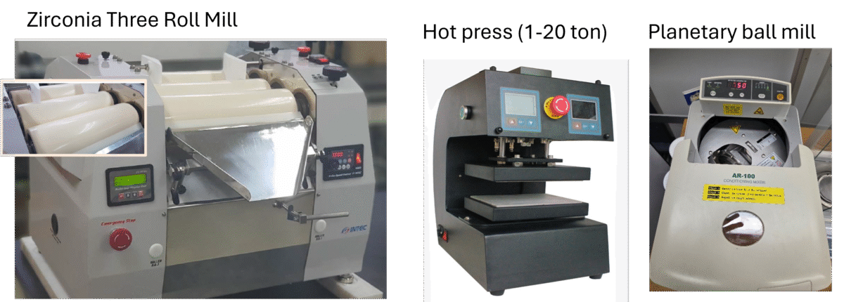
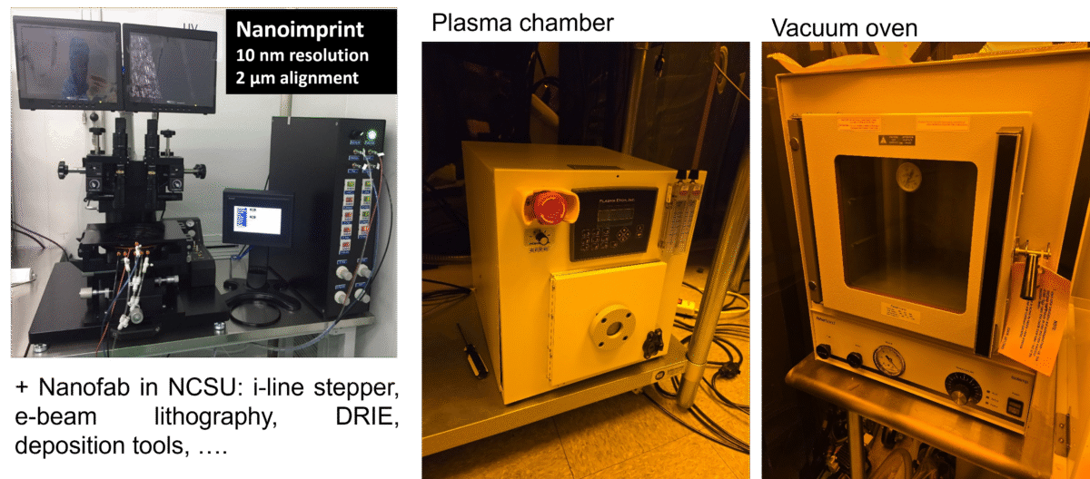
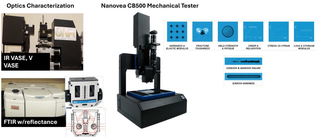
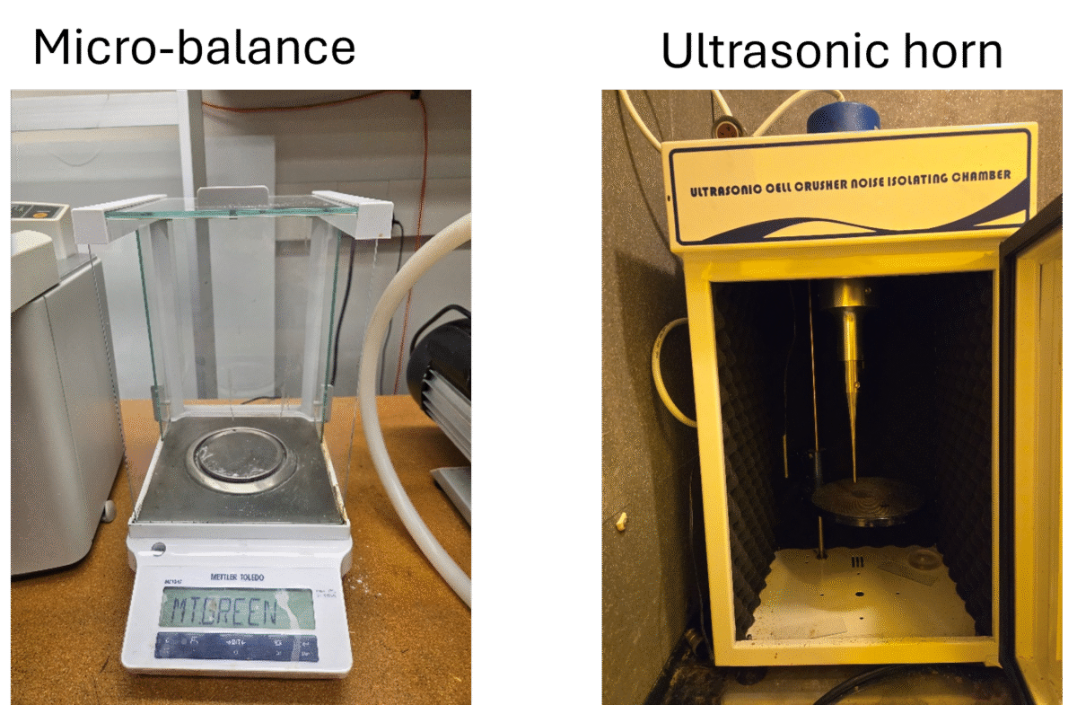
LAB EQUIPMENT