
Power Electronic Packaging and Reliability
Power electronics are the backbone of modern technology, converting and controlling electric power to efficiently operate everything from electric vehicles and renewable energy systems to consumer electronics. As devices become smaller and more powerful, vertical integration and 3D heterogeneous integration are the latest trends in power electronics technology. This involves stacking and interconnecting different components, such as power devices, drivers, and capacitors, to create highly compact and efficient modules.
This integration, while powerful, presents significant reliability challenges. The complex interplay of thermal, mechanical, and electrical stresses—known as multiphysics interactions—can lead to novel failure modes. These interactional failure driving forces require new approaches to design and analysis. To address this, co-design—the simultaneous optimization of device, package, and system—and digital twin technology are becoming crucial. A digital twin is a virtual replica of a physical system that allows for real-time monitoring and predictive analysis of reliability, making it an indispensable tool for developing complex 3D power integrations.
The advent of wide-bandgap (WBG) devices, such as those made from Silicon Carbide (SiC) and Gallium Nitride (GaN), has further pushed the boundaries. These devices operate at higher temperatures and frequencies than traditional silicon, making them ideal for harsh environments like those found in space, supersonic applications, or high-temperature industrial settings. This shift has made power electronics research more critical than ever, focusing on creating robust packages that can withstand extreme conditions.
Our Laboratory and Facilities
Our laboratory is equipped to perform comprehensive power electronics package assembly and analysis, addressing the full spectrum of challenges in modern power electronics.
Assembly
We have a close collaboration with the Packaging Research in Electronic Energy Systems (PREES) lab at NCSU, where Dr. Ryu serves as an Associate Director. The PREES lab is fully equipped to perform power electronics assembly on various substrates, including PCB (Printed Circuit Board), DBC (Direct Bonded Copper), and IMS (Insulated Metal Substrate).
PREES Lab
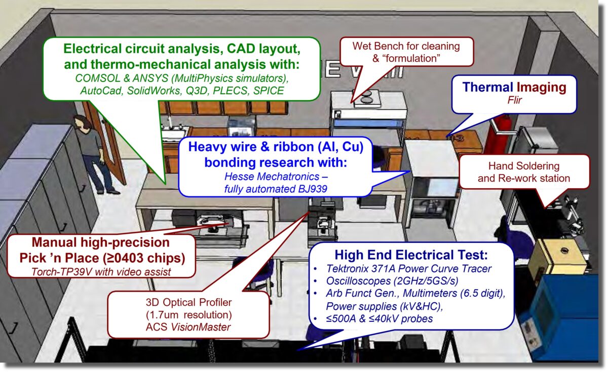
Key equipment includes:
- Semi-manual pick-and-place machine
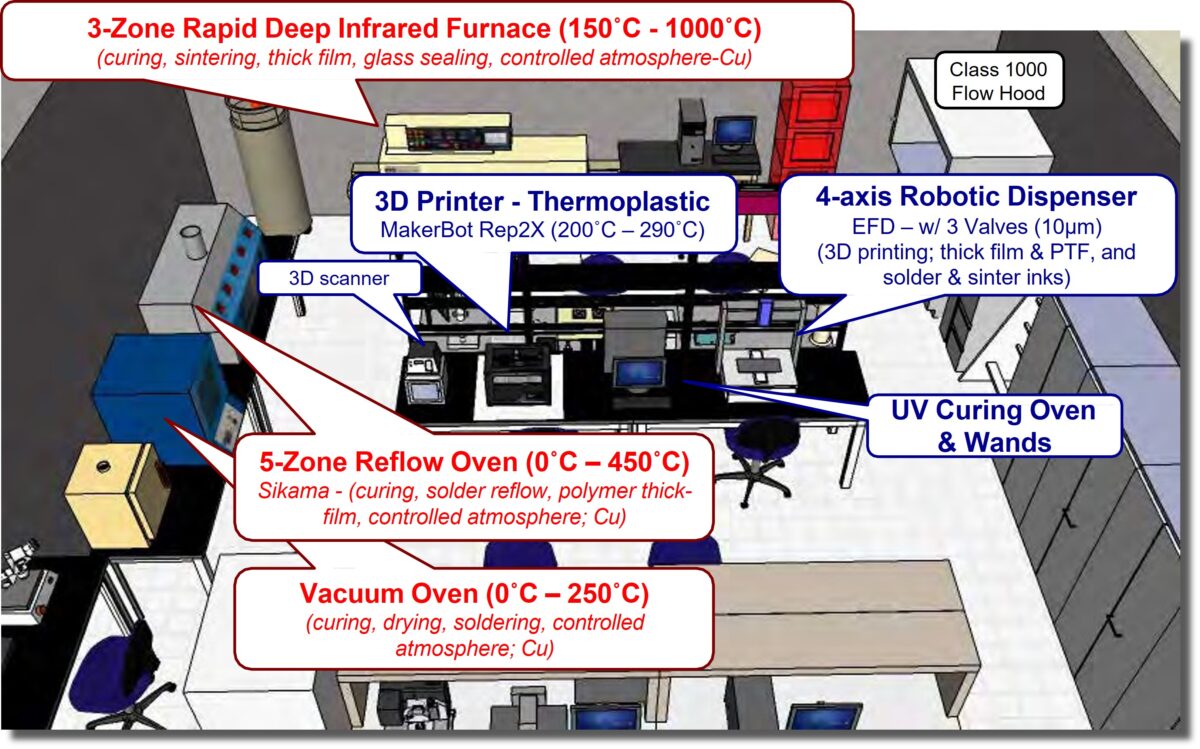
- 5-zone reflow oven
- IR 3-zone sintering furnace
- 4-axis 10-μm resolution Engineered Fluid Dispensing (EFD) system
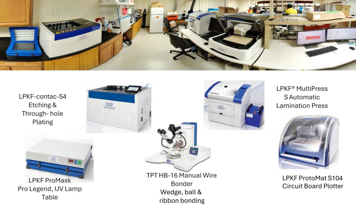
- Heavy wire and ribbon (Al, Cu) bonder
- Through-hole electroplating
- PCB lamination press
- Solder mask print and coating
- Circuit board plotter (micro-mill)
Additionally, we utilize the NCSU Additive Manufacturing facility for 3D printing of polymer, metal, and ceramic components, enabling the creation of custom, complex structures for advanced packaging.
Test and Characterization
Our testing and characterization facilities allow for detailed analysis of material properties and device performance.
Material Characterization:
- Micro/nano-scale mechanics: micro-indentation and nano-indentation for mechanical property characterization.
- Adhesion and bonding strength: Universal testing machine to measure adhesion and bonding strength.
- Physical properties: Physical Property Measurement System (PPMS) to measure thermal conductivity, electrical resistivity, and thermal expansion coefficient.
- Nano-scale surface characterization: Scanning electron microscope (SEM), Atomic force microscope (AFM), transmission electron microscope (TEM), and Focused Ion-Beam (FIB) milling for high-resolution surface analysis.
Device Performance Measurement:
- Power curve tracer
- Oscilloscope
- Function generator
- Probe station
Simulation and Computation:
- Workstations and access to the NCSU High-Performance Computing (HPC) facility.
- Licensed software including ABAQUS, ANSYS, and COMSOL for multiphysics simulations.
Selected Publications
- “Digital Twins for IC Packages and Electronics-enabled Systems.” 2024 IEEE Smart World Congress (SWC). IEEE, 2024.
- Design, Fabrication, and Operation Challenges of Advanced Power Packaging Technology for EV Power Modules. 2025 IEEE International Workshop on Integrated Power Packaging (IWIPP). IEEE, 2025.
- Innovative Packaging Strategy for MLCCs for High Current AC Applications Aimed at Reducing Parasitic Inductance. 2025 IEEE International Workshop on Integrated Power Packaging (IWIPP). IEEE, 2025.
- Co-Design and ML-Based Optimization of Through-Via in Silicon and Glass Interposers for Electronic Packaging Applications. IEEE Transactions on Components, Packaging and Manufacturing Technology (2025).
- Deep Neural Network-Based Temperature Mapping Technique for Heat Sink on Electronic Devices Using Local Thermocouple Sensors. Applied Artificial Intelligence 38.1 (2024): 2389374.
- “Investigation of High Current Fine Grain Power Delivery for 3D Heterogeneous Integration.” IEEE Transactions on Components, Packaging and Manufacturing Technology (2024).